The AMDAHL 5860 had a 24 nanosecond machine cycle time with a bus width of 72 bits - 64 data bits and 8 bits of parity. Keep this bus width in mind when you compare the VLSI processor chips that obsoleted the mainframe, they had a bus width of just 8 bits but much, much faster, because of shorter interconnections.
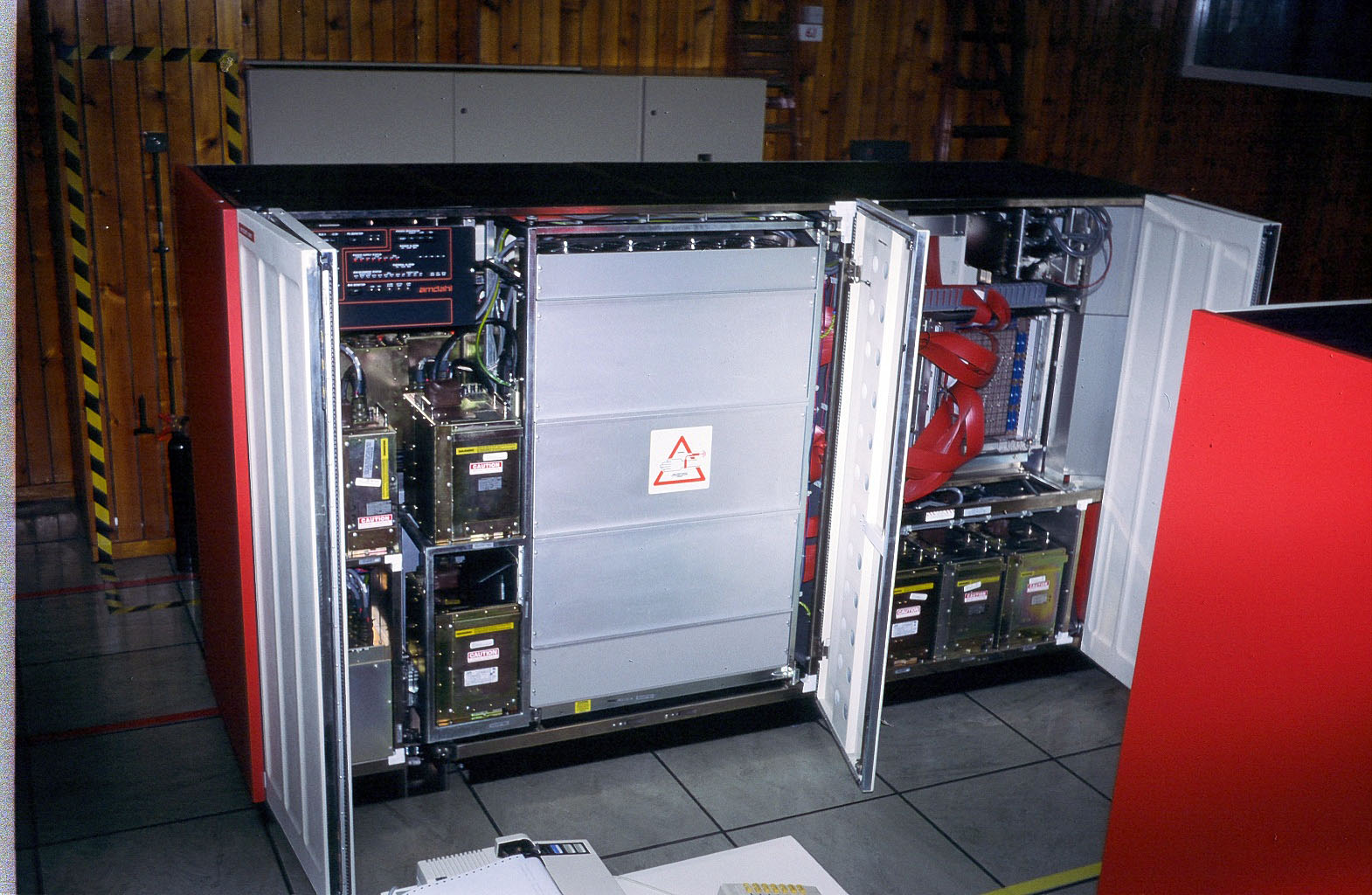
To the right is a gate containing 40MByte of RAM.
To the right of that is the CPU (Central Processing Unit),
called The Stack and below it its power supplies.
The Stack was connected by the large red ribbon cables
to the RAM and I/O channels.
We have one of the power supplies described Here
We have The Stack in the collection.
| Mus.Cat: NEWUC:2003.19 | Mnfctr: AMDAHL | Date: 1985 | Ser. No: 365 | Model: 5860 |
| Comp: CPU | Length: 600 mm | Width: 480 mm | Depth: 640 mm | Weight: 96 Kg |
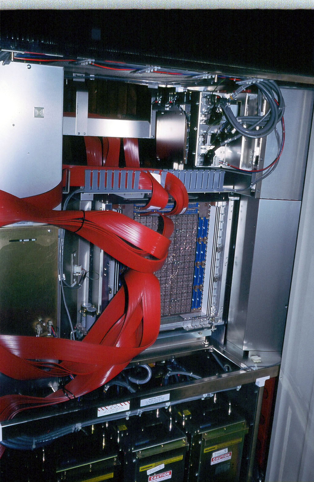
To the right and at the bottom can be seen three of the bus-bars that delivered electricity to the Stack.
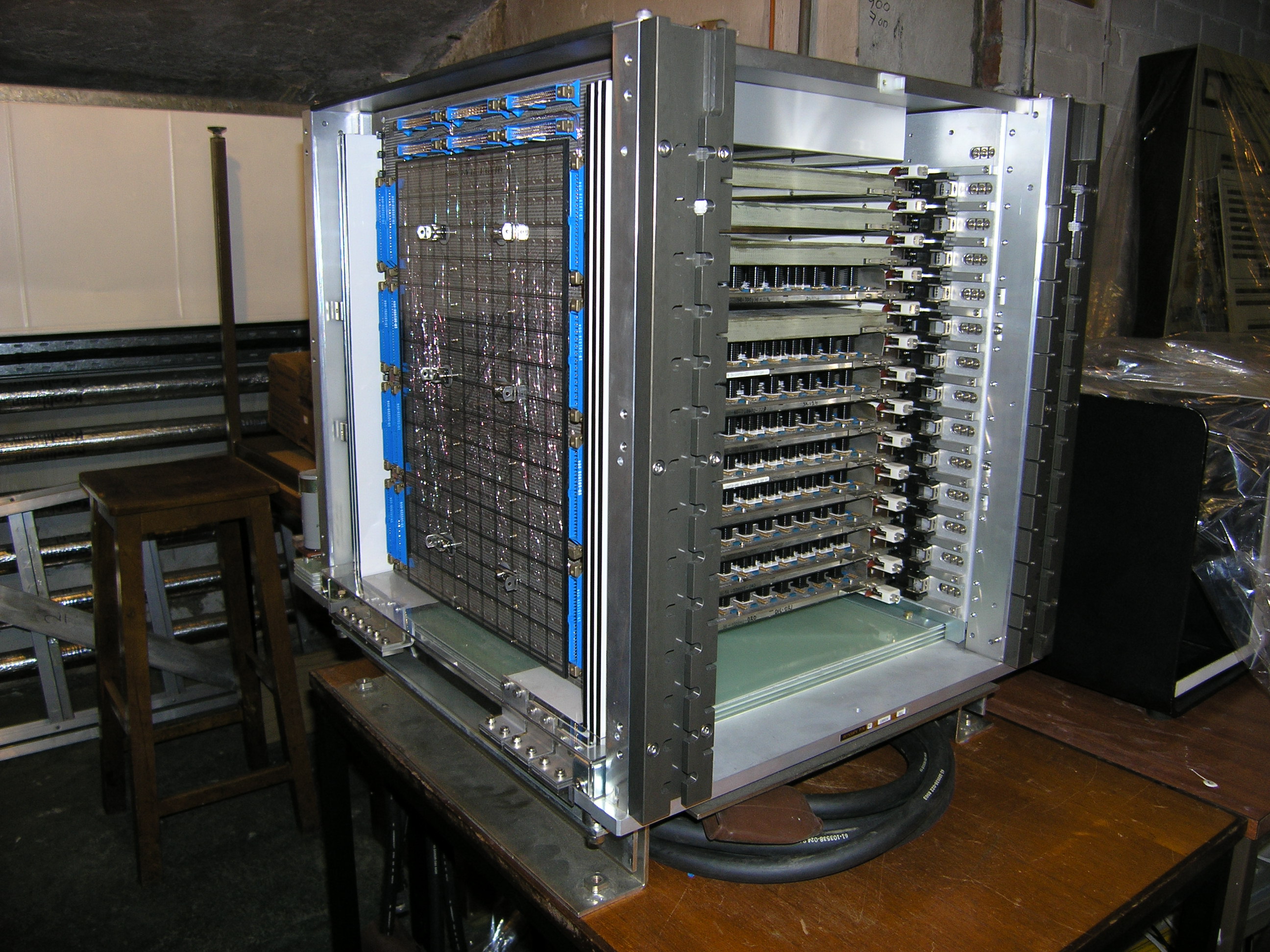
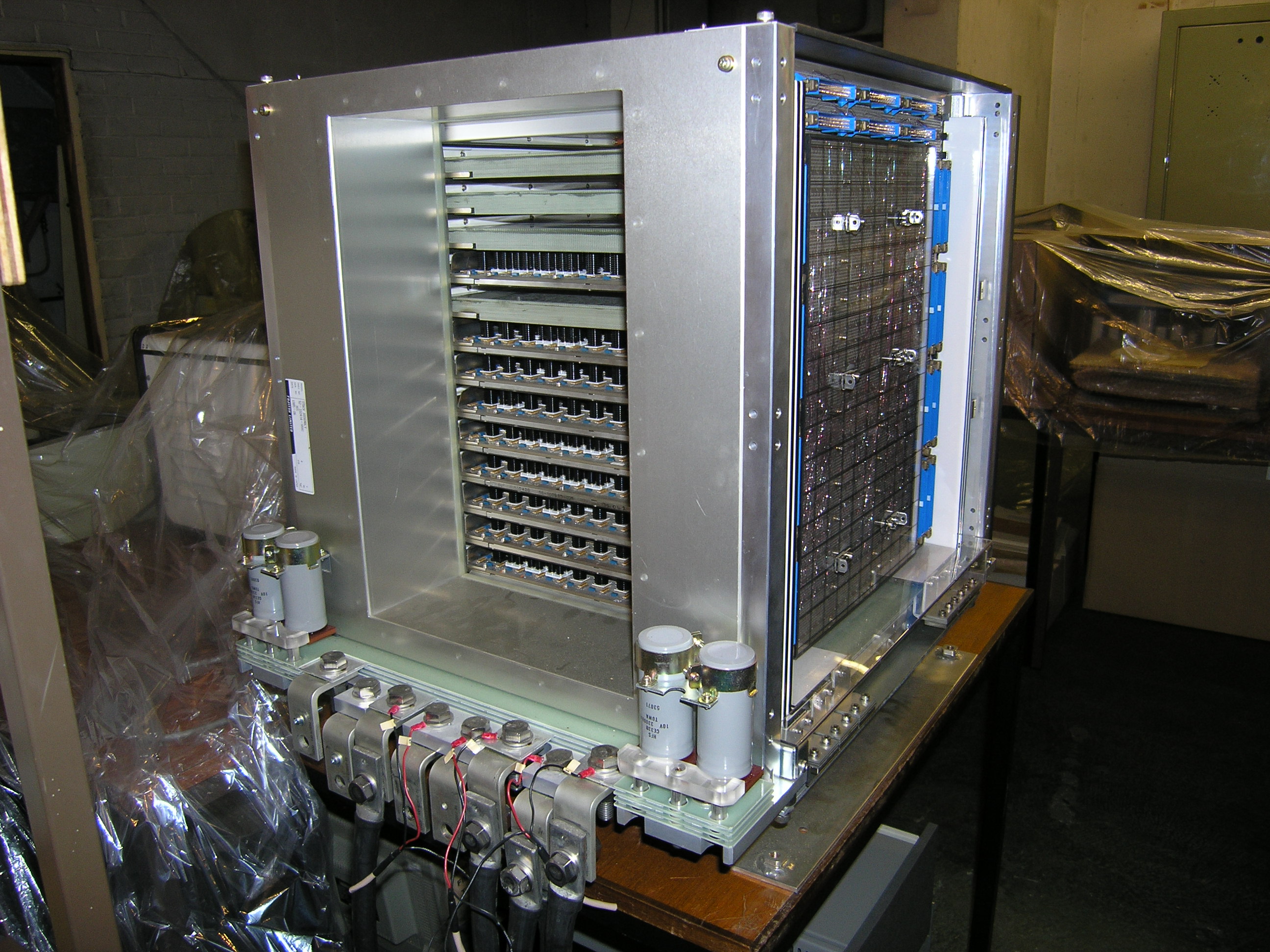
In the AMDAHL 5860 the boards were one above the other connected by two busses, 12 layer printed circuit boards one on each side, meaning shorter connections, meaning faster speed.
they are from top to bottom:BLANK
BLANK
BLANK
Console Subsystem
BLANK
Input/Output Processor
Memory Bus Controller
Storage Unit
Buffer Unit
Instruction Unit
Execution Unit
Floating Point Unit
In the end the Amdahl was unceremoniously craned from the computer room, cabinet by cabinet, into, big, battered, dirty wagons, with no care and driven off in a haze deisel fumes.
We had treated the Amdahl almost with reverence just to touch it was an privilege to actually open it up and pull bits out was unthinkable except to the Amdahl engineers.
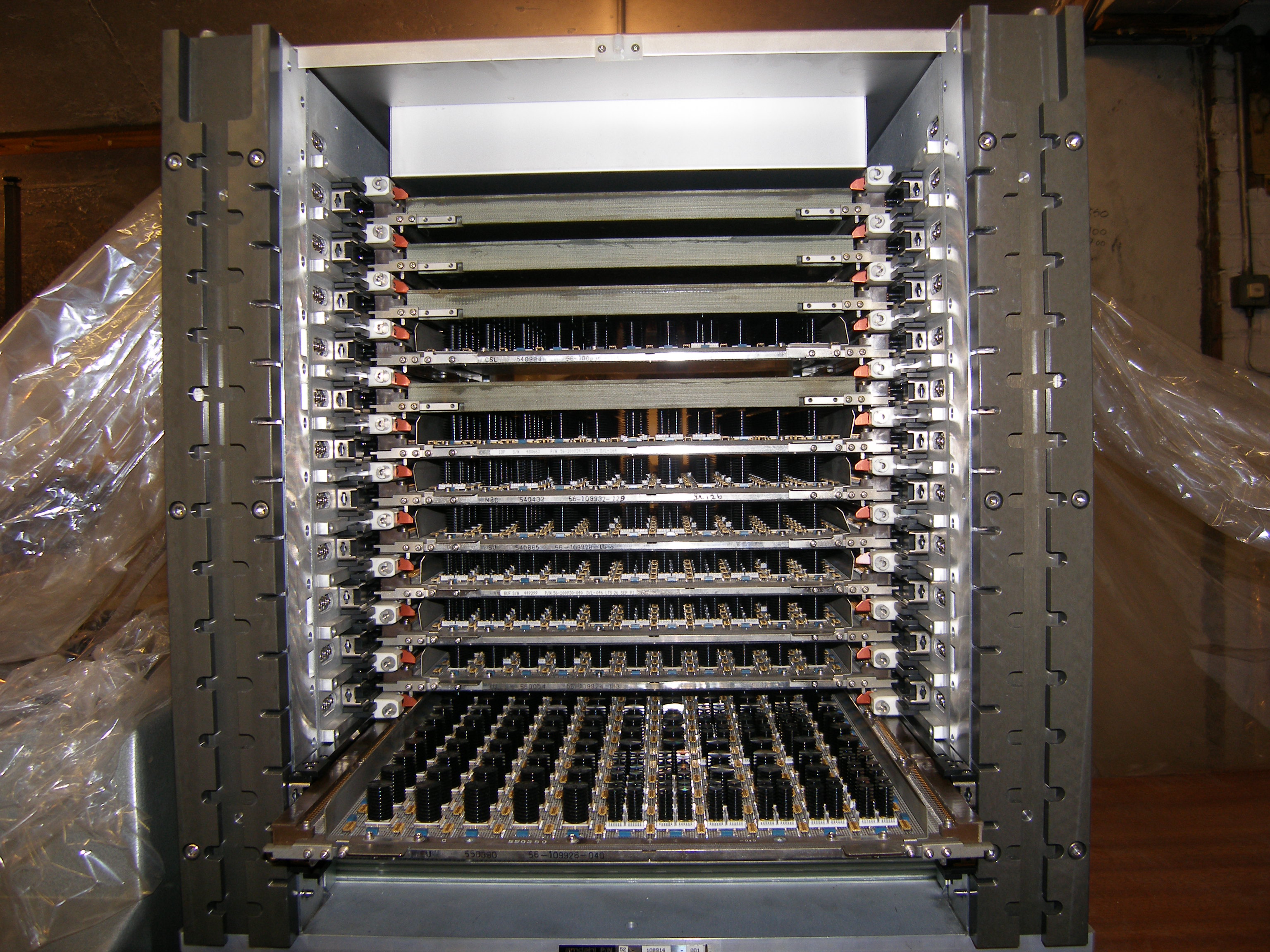
The boards were called MCCs (Multiple Chip Carriers) are 14 layer printed circuit boards that accomodated both LSI RAM and Logic chips to implement an entire system function. The LSI RAM chips, (with an access time of 7.5 nanoseconds - 133 Mhz), provide storage for registers, buffers, and control stores. The Logic chips contain 400 circuits and have an average switching time of 400 pico seconds.
The Stack could accommodate twelve boards so four board places were replaced with Bakelite blocks, because the whole Stack had chilled air blown through it to take away the heat and the designers did not want the chilled air to go through the vacant spaces. They wanted it to go through the spaces between the boards where the 'black' cylinders are.
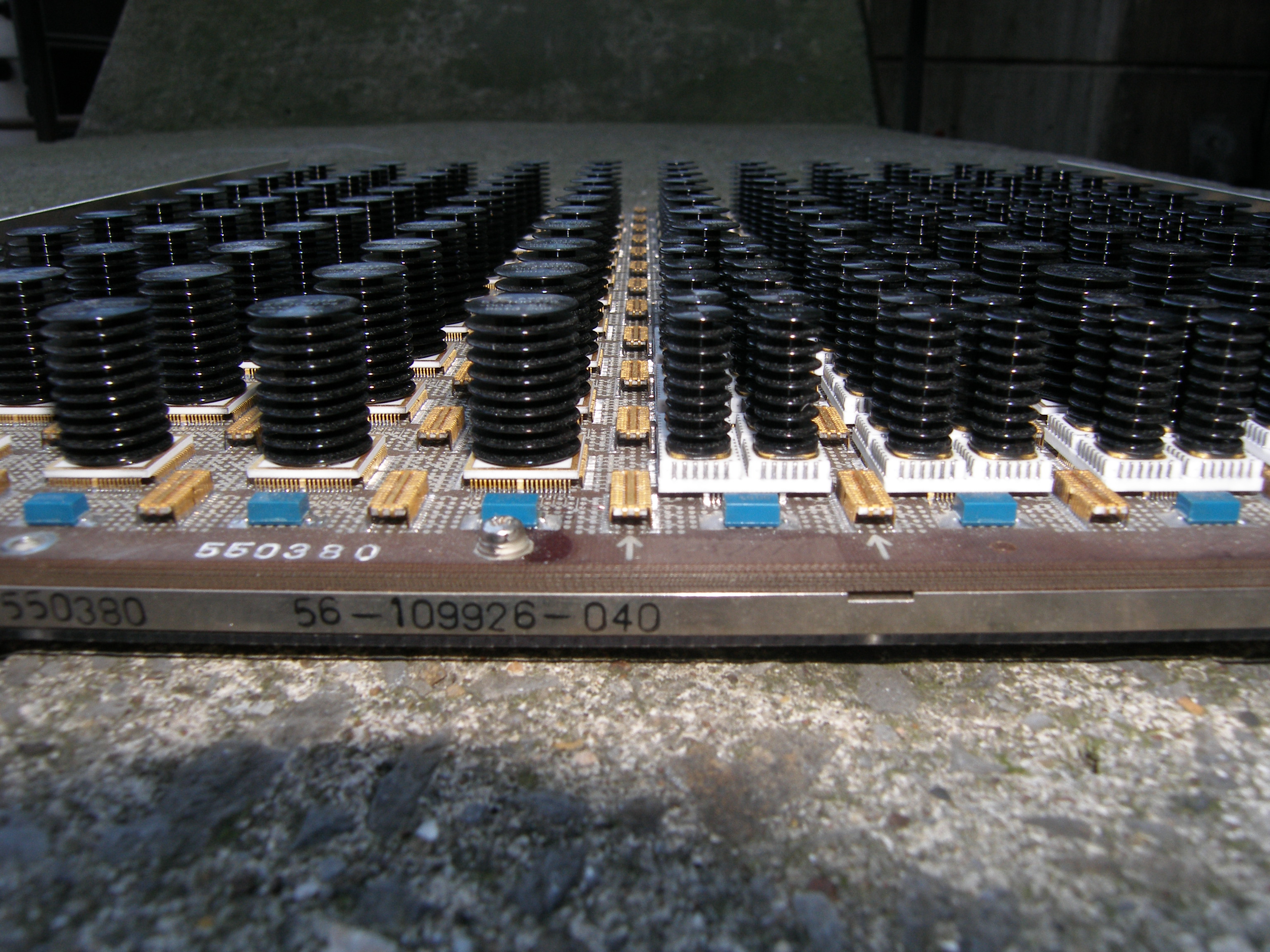
The chips on the right with four narrow heat sinks are LSI RAM chips. Those on the left with a single large heat sink are Logic chips.
The chips use Emitter Coupled Technology, which though fast, used a lot of electricity, so generated a lot of heat that had to be dispersed.
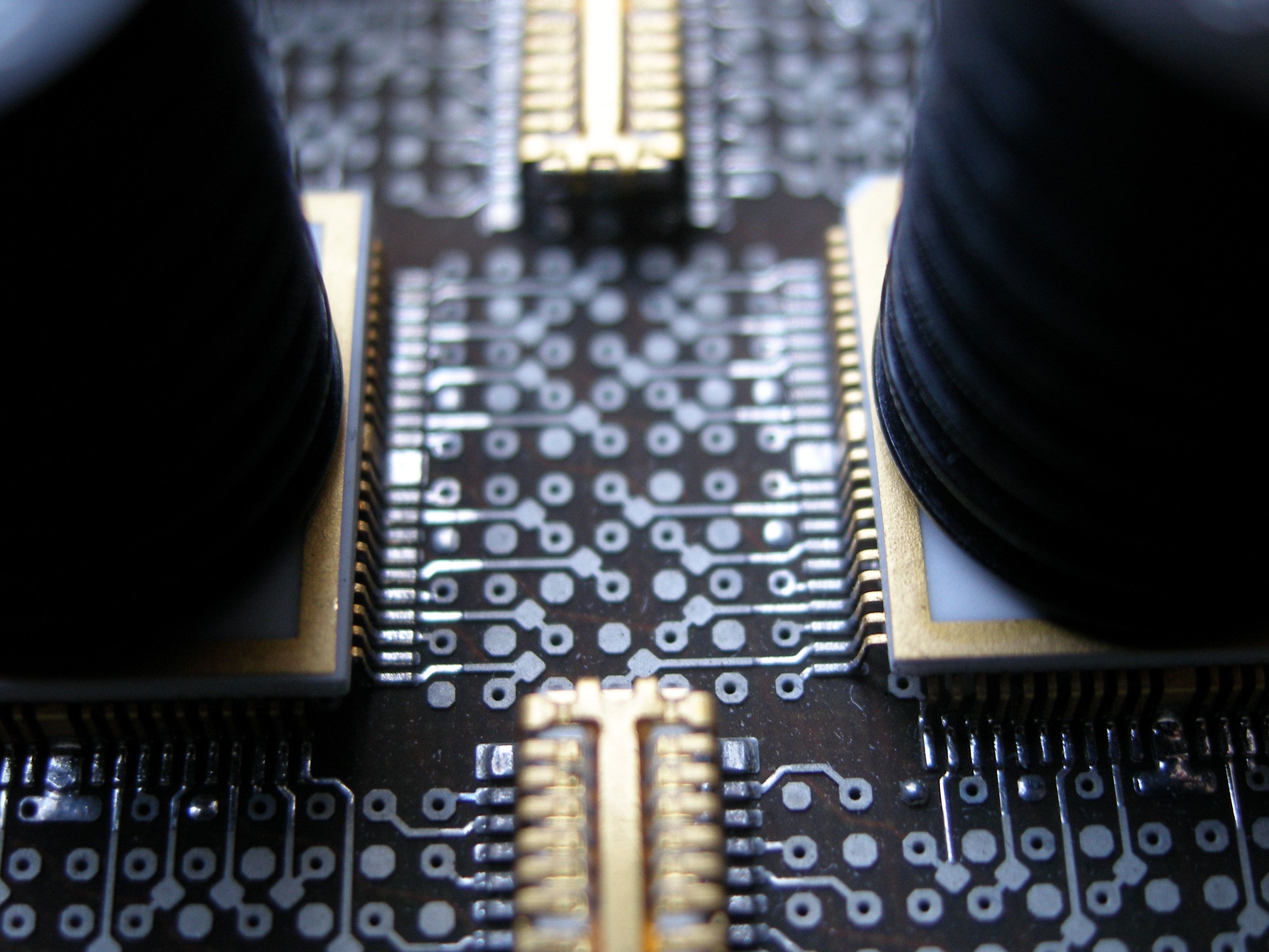
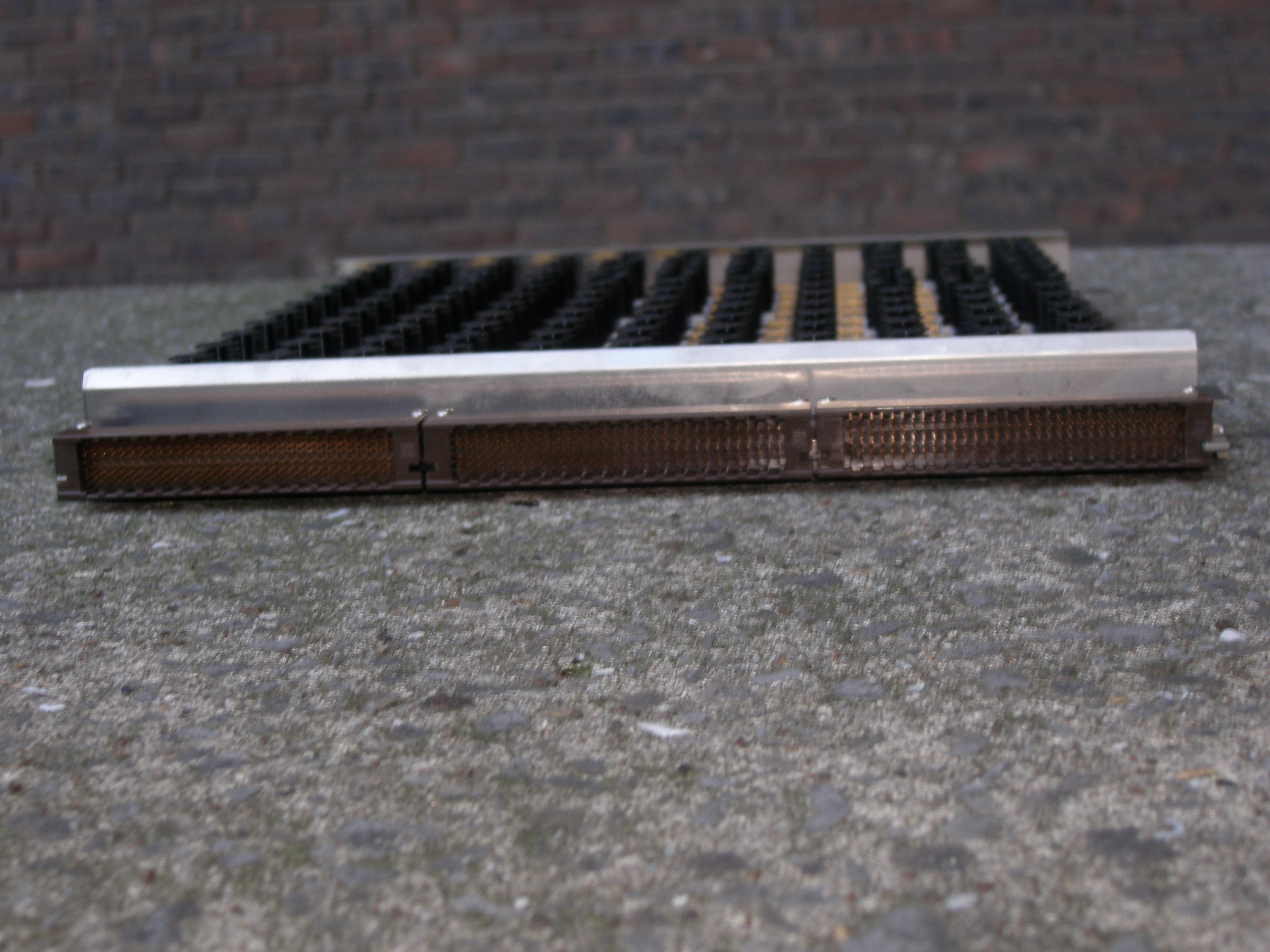
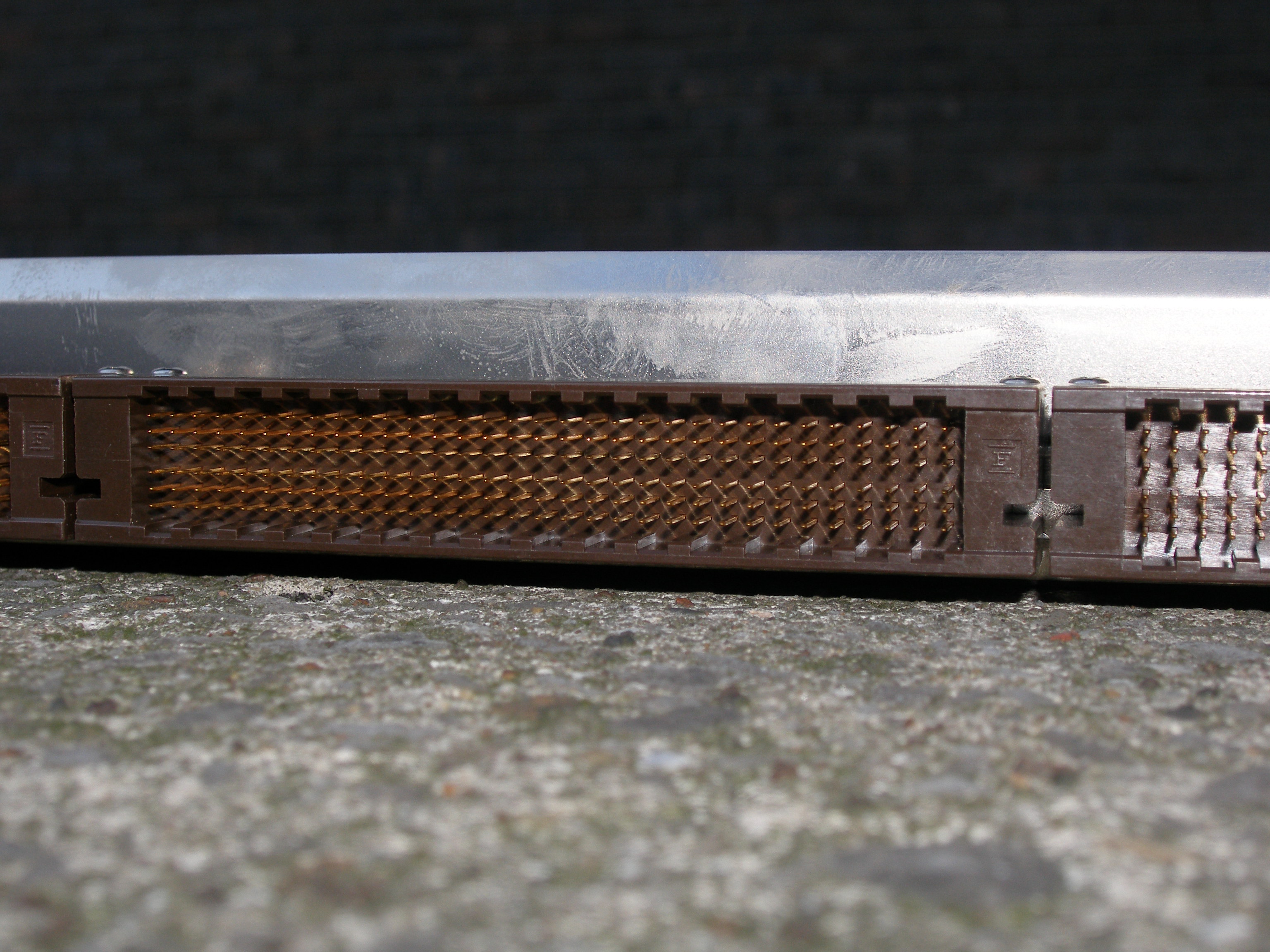
This is a photograph of the side of the board there are three blocks of connections on each side. Bear in mind these are the sides of the boards when it is inserted into the body of the Stack. How are the connections made?
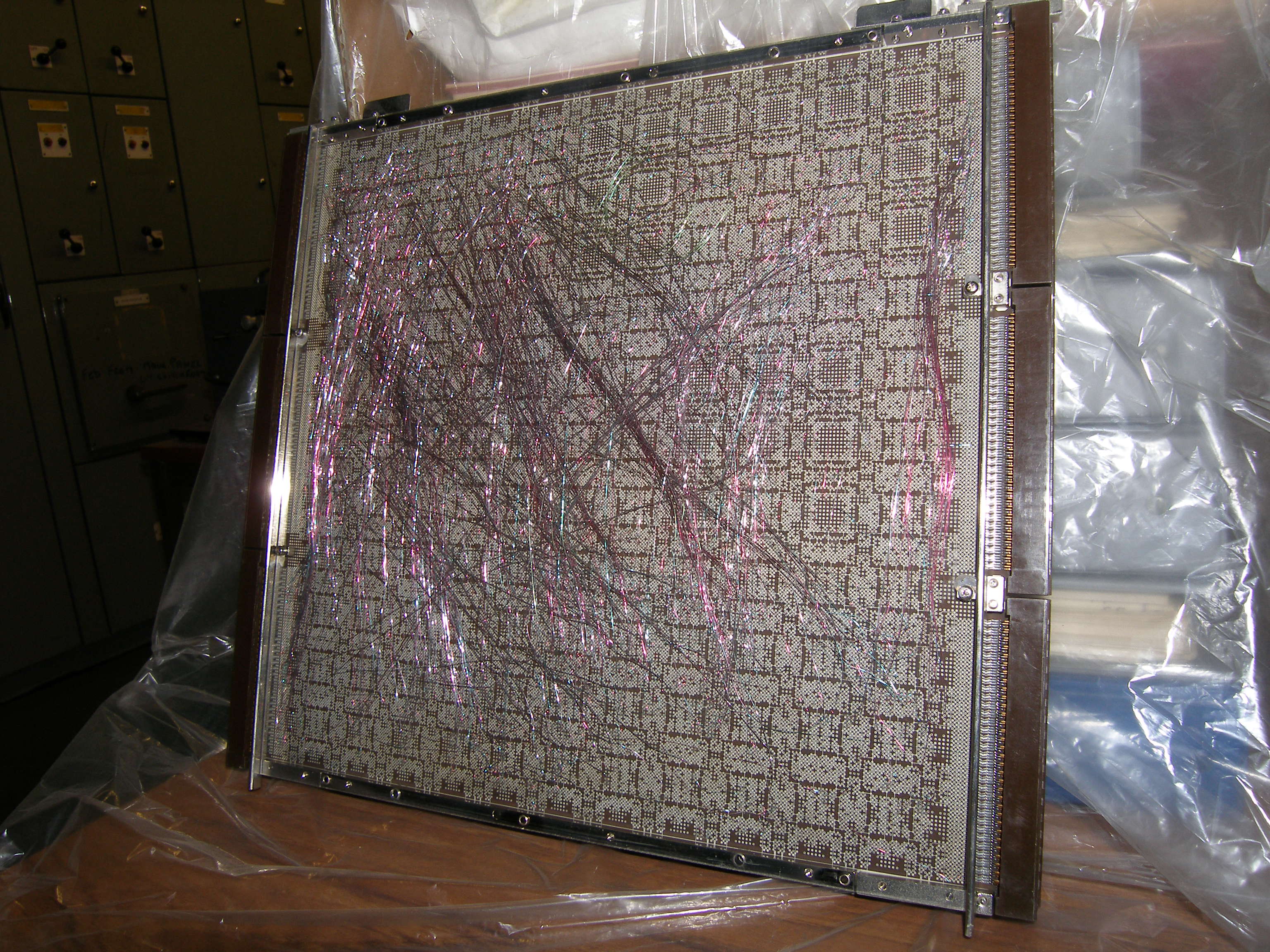
This is a rear view of the 14 layer printed circuit board, but still needed a deal of back wiring.
Each board measured 11" x 13" and could accomodate 121 LSI chips (over 48,000 circuits).
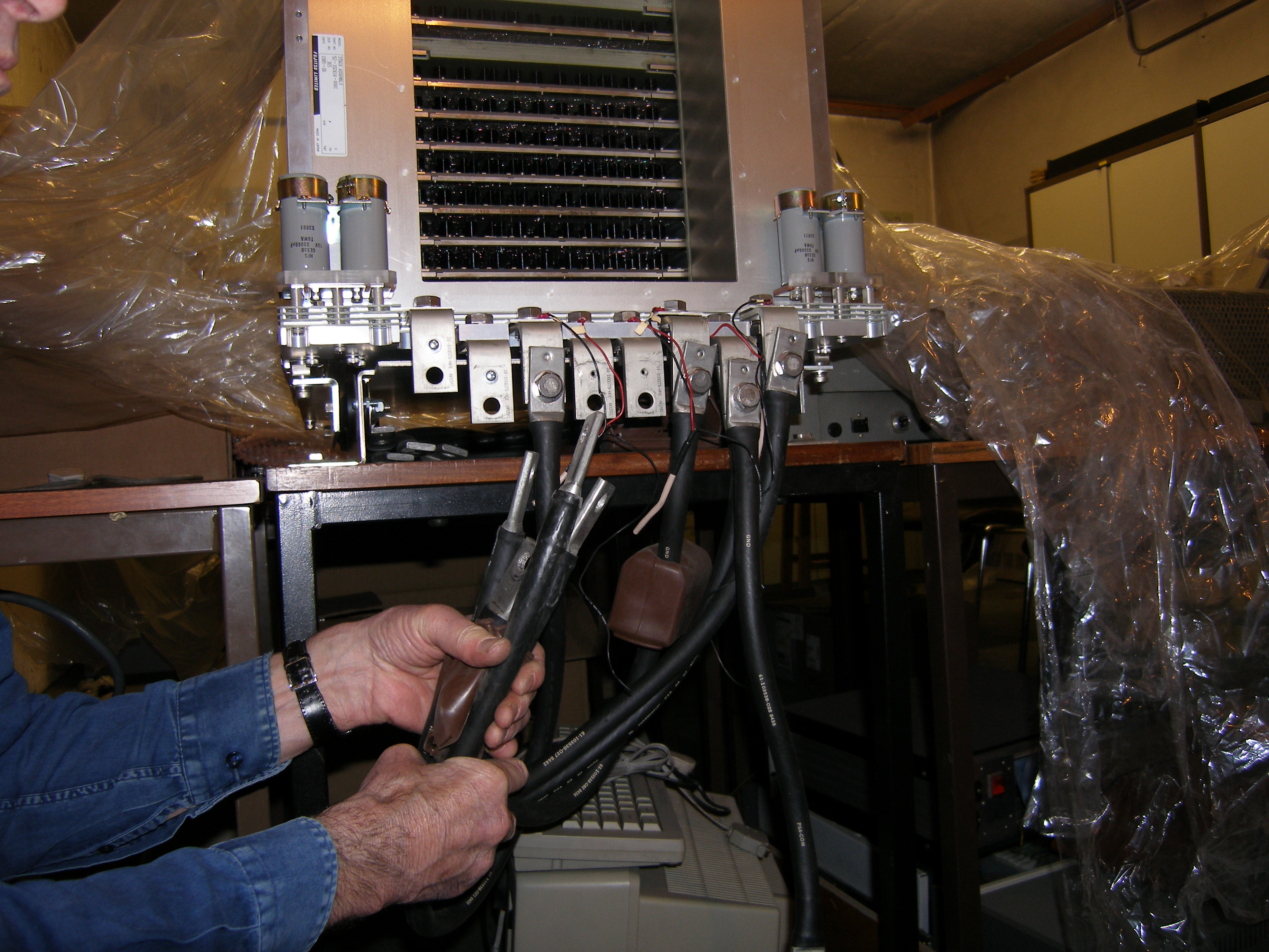
This is the rear of the Stack. At the bottom is the connectors for the power cables.
There are nine bus-bars each heafty bits if copper.
On the left side is a label ...
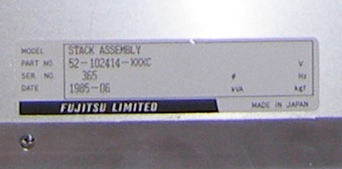
Here it is, enlarged and rotated. It says:
| MODEL | STACK ASSEMBLY | ||
| PART NO | 52- 102414- )00( C | V | |
| SER NO | 365 | # | Kg |
| DATE | 1985-06 | kVA | k?? |
There is interesting information here. Unfortunately not the weight or power KVA consumption.